Home![]() Research description
Research description![]() Theme IV
Theme IV
Research description
Theme VI. Polariscopic analysis for strains in semiconductor single crystal wafers
Solid-state physics and classical optics have the ability of rapidly and reasonablely inspecting emerging semiconductor single crystal wafers.
Applicable to improvement of yield rates in mass production of emerging semiconductor single crystal wafers for device substrates.
1 : Summary of outline, objectives and outcomes
Viewgraphs (in English) ... see the presentation materials
Wide band-gap semiconductors, which are well regarded as important materials for optoelectronics, have also been receiving much attention in the field of power electronic devices and components because of their advantages in realizing a high breakdown voltage. In the mass production of the semiconductor wafers use for the substrates, it is essential to increase a yield rate; however, the issues on the yield rate are not completely solved. The issues result from the fact that growth technologies for the wide band-gap semiconductor wafers quite differ from those of traditional GaAs, InP, and Si wafers. The GaAs, InP, and Si wafers are grown using liquid-to-solid phenomena. The technique based on the liquid-to-solid phenomena is well established. In contrast, the growth technologies for the wide band-gap semiconductor wafers are state-of-the-art, comparing with the wafer-growth technologies for GaAs, InP, Si, and so on. The SiC wafers are made with use of sublimation methods: the crystallization from the gas phase to solid phase. The GaN wafers are fabricated by hydride vapor-phase epitaxy. For the growth of the ZnO wafers, a hydrothermal method is employed. The referenced growth technologies are the emerging wafer-growth methods; namely, the growth technologies for the wide band-gap semiconductor wafers do not reach a well-established status. It is, therefore, necessary to control quality of the mass production of the wafers. The above-described background indicates that it is significant to explore the reasonable and suitable characterization methods for the mass production. It is, of course, fundamental that the characterization is nondestructive.
We focus our attention on exploring convenient and the high throughput characterization/inspection technology for internal and/or residual strains of the wide band-gap semiconductor wafers because the relatively large strains sometimes lead to the fragility and resulting cracks. Accordingly, it is essential to the suppress the crack in obtaining the high yield rate. In addition, the internal strain usually is concerned with the crystal misorientation of the wafers, on which epitaxial layers are grown. There have been various characterizing technologies for evaluating the internal strains such as photoluminescence spectroscopy and Raman scattering spectroscopy. The referenced spectroscopic characterization has been widely utilized in the research and development of the crystal growth. In addition, the x-ray diffraction measurement and x-ray topography are also regarded as the useful characterizations. On the other hand, we wonder whether the above-mentioned evaluation measurements satisfy the demand from the wafer mass production because these measurements require the relatively long time for the evaluation, leading to the low throughput. The wide band-gap semiconductors are transparent to the visible light, so that the analysis of the transmittance light has the ability of the precise strain evaluation. Polariscopy, which utilizes photoelastic effects resulting from the stains, is a measuring method on the basis of the fundamental characteristics of light: polarization. In the inhomogeneous materials where the stain effects are dominant, the light which transmits from the sample under the test, exhibits the optical birefringence owing to formation of fast and slow axes. This causes the change in the direction of the polarization. We present the evidence that the polariscopic analysis has a high sensitivity, compared with the Raman scattering and photoluminescence measurements.
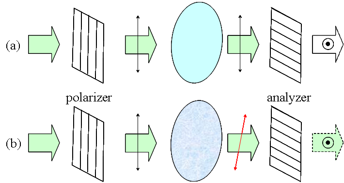
Figure 1: Explanation of the photoelastic phenomenon and concept of the polariscopic measurement.
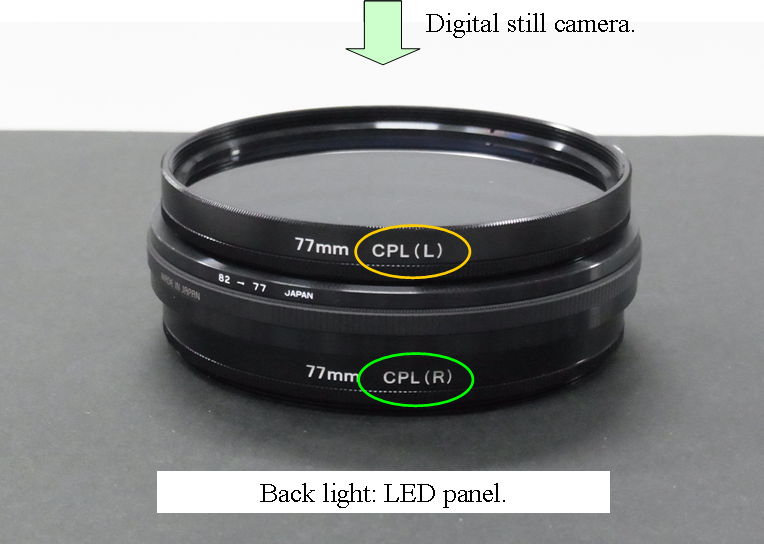
Figure 2: Experimental setup for the polariscopic measurement.
The fundamental concepts of the photoelastic effects and the experiment setups for the polariscopic measurements are shown in Figures 1(a) and 1(b). As shown in Figures 1(a) and 1(b), the polarizing plates which used for the polarizer and analyzer, are in the perpendicular alignment, the cross-Nicol configuration (sometimes referred as cross-Nicoled configuration). The sample under the test is inserted between the polarizer and analyzer. Figure 1(a) schematically shows the case where the sample free from the strains is under the test. In the condition shown in Figure 1(a), the sample is optically isotropic because the symmetry of the crystal does not change. The direction of the polarization of the light is kept and the light cannot transmit from the analyzer. Figure 1(b) shows the sample that contains the strains. The strains lower the crystal symmetry. The lowering of the symmetry is explained in terms of the fact that the lattice constant is deviated from that of the ideal crystal. The above-mentioned phenomenon produces the optical fast and slow axes: the photoelastic effects The production influences the polarization of light and changes the direction, so that the some part components of the light transmitted from the sample is allowed to pass through the analyzer. This is observed as the distributed brightness in the transmittance image. In usual, for the isotropic crystal with a symmetry Td (F43m), linear polarization optics is used. In the crystal with a symmetry such as C6v4 (P63mc), the polariscopic measurement is applicable with use of the left and right circular polarization optics, of the evidence which is shown in Sections III and IV. Figure 2 shows the example of the setup for the polariscopic measurement in the cross-Nicol configuration. The experiment apparatus is quite simpler than those used for other crystal characterization methods. The light source is a white light-emitting-diode panel. The image, reflecting the intensity of the light transmitted through the analyzer, is recorded with use of a conventional digital still camera. The sample is inserted between the polarizer and analyzer. The polarizing plates used for the polarizer and analyzer are conveniently available Polaroid films.
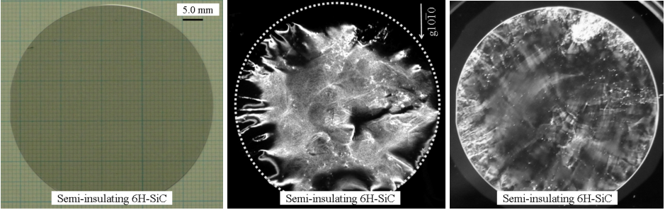
Figure 3: (from left) (a) Optical photograph, (b) transmittance-type x-ray topograph, and (c) circular polariscopic map of a 2-inch-size (0001)-oriented semi-insulating 6H-SiC wafer.
We present the ability of the polariscopic analysis for the strains in semiconductor wafers. Figues 3(a), 4(b) and 4(c) show the optical photograph, transmittance-type x-raytopograph, and circular polariscopic map, respectively. In Fig. 3(b), the undulation of the x-ray topograph, which is recorded as a change in brightness, reflects the disturbance of the magnitude of the crystal-axis orientation. The region, which is dark, corresponds to the low orientation. This means the occurrence of the misalignment. In general, the crystal quality of semiconductor wafers around the center is better than the crystal quality near the edge. The x-ray topograph image extinguishes near the wafer edge. The dark patterns exist in various regions. Consequently, it is impossible to obtain the information on the condition near the wafer edge.
The circular polariscopic map of the sample is shown in Fig. 3(c). The circular polariscopic map clearly reflects the condition of the whole wafer as the brightness corresponding to the magnitude of the strain. The present circular polariscopic map was obtained within 1 sec, so that the present method has a high potential to conveniently evaluate the strain distribution in comparison with the x-ray transmittance topographic measurement. Thus, the circular polariscopic analysis has the ability to complement the monochromatic x-ray topographic analysis applied to the SiC wafer mass production.
We also show the result obtained from the application of the polariscopic measurement to a (0001)-oriented ZnO wafer. The elements of Ga and Zn have a high x-ray absorption coefficient, so that the conventional transmittance-type x-ray topographic measurement is inappropriate to the wafers of the Ga-X or Zn-X crystals, where X denotes other elements: Oxygen, nitrogen and so on.
The transmittance-type x-ray topographic images of a 2-inch-size (0001)-oriented ZnO wafer is shown in Fig. 4(b). It is apparent that the transmittance monochromatic x-ray topograph is strongly noisy. The phenomenon originates from the fact that the element of Zn has a high x-ray absorption coefficient. This suppresses the x-ray transmittance and, as a result, results in the noisy image.
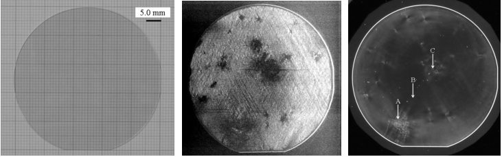
Figure 4: (from left) (a) Optical photograph, (b) transmittance-type x-ray topograph, and (c) circular polariscopic map of a 2-inch-size (0001)-oriented ZnO wafer.
The circular polariscopic map of the sample is shown in Fig. 9(c), in which the condition of wafers are clarified without noise. Regions A and C, which exhibit grain-like patterns in the x-ray topograph, are bright. In contrast, region B is dark. The phenomena, which are observed both in the x-ray topograph and in the circular polariscopic map, indicate that the crystal quality is lowered in regions A and C. The present findings indicate the high sensitivity of the polariscopic measurement. The polariscopic analysis is, therefore, an effective method for evaluating wide-band-gap semiconductors transparent to the visible light.
The research activities on the polariscopic analysis brought the following 5 papers
2 : List of outcomes
Publications
5
"Comparison in Internal Strain Sensitivity between Polariscopy and Raman Scattering Spectroscopy
in a (110)-oriented ZnTe Single Crystal".
Hideo Takeuchi,
Physica Status Solidi C (2014) in press.
#
Link to the online-journal site
4
"Enhancement effects on excitonic
photoluminescence intensity originating from misaligned crystal
blocks and polycrystalline grains in a ZnO wafer".
Hideo Takeuchi
The European Physical Journal B 86:50 1-5 (2013).
#
Link to the online-journal site
3
"Circular polariscopic analysis of a
ZnO wafer for highly sensitive and speedy evaluation of residual
strains: Its relation with x-ray diffraction pattern and
topography ".
Hideo Takeuchi.
Physica Status Solidi C vol.9, pp.1817-1820 (2012).
#
Link to the online-journal site
"Circular polariscopic analysis of a
ZnO wafer for highly sensitive and speedy evaluation of residual
strains: Its relation with x-ray diffraction pattern and
topography ".
Hideo Takeuchi.
Physica Status Solidi C vol.9, pp.1817-1820 (2012).
#
Link to the online-journal site
1
"Circular polariscopic analysis of
strains in a semi-insulating SiC wafer: Its high potential to
complement the information obtained from monochromatic x-ray
topography".
Hideo Takeuchi.
Review of Scientific Instruments vol.82, 033907 1-5 (2011).
#
Link to the online-journal site
3 : Posters and viewgraphs
1 "Intense emission of THz electromagnetic wave from an undoped GaAs/n-type GaAs epitaxial layer structur".
H. Takeuchi, J. Yanagisawa, T. Hasegawa, and M. Nakayama.
The 35th International Symposium on Compound Semiconductors (ICSC2008) September 21-24, 2008, Europa-Park, Rust, Germany.
*** Poster Presentation P34 (September 23, Tuesday) ***
The abstract is here. The poster is here.
2 "Direction reversal of the surface band bending in GaAs-based dilute ni-tride epitaxial layers investigated by polarity of terahertz electromagnetic waves".
Hideo Takeuchi, Junichi Yanagisawa, and Masaaki Nakayama.
The 14th International Conference on Narrow Gap Semiconductors and Systems (NGSS-14) July 13-17, 2009, Sendai, Japan.
*** Oral Presentation: Talk-8 (July 15, Wednesday) ****
The abstract is here. The viewgraph is here.