Home![]() Profile
Profile
Profile
Hideo Takeuchi was born in January 8, 1973. Place of Birth is Otsu city, Shiga prefecture, Japan, near the famous city, Kyoto. His educations and work experiences are full of variety. He always says, "What a difference a day makes".
In the present page, he introduces his experiences as "Phases" in order of increasing year. Someone wonders why he uses the term, phase. This is simply because he is deeply interested in variou oscillatory phenomena, the fundametals of physics :-).
Education and Professional Experience
Phase 1|Apr. 1991 to Mar. 1995: Osaka City University (1st term)
![]()
He was in Department of Applied Physics, Faculty of Engineering, Osaka City University with a bachelor's ( BA ) degree in Engineering.
Bachelor thesis : Optical properties of CuCl and CuBr crystalline thin films grown by vacuum deposition.
He was a member of the Laboratory of the Optical Properties and Functions of Materials . He studied the excitonic properties of the CuCl and CuBr thin films. He set up the vacuum-evaporation machine for the thin films with his collaborators. He also intensively performed the following spectroscopic measurements: absorption, photoluminescence, and photoluminescence-excitation spectroscopy.
Phase 2|Apr. 1995 to Mar. 1997: Osaka University
Department of Physics, School of Science
![]()
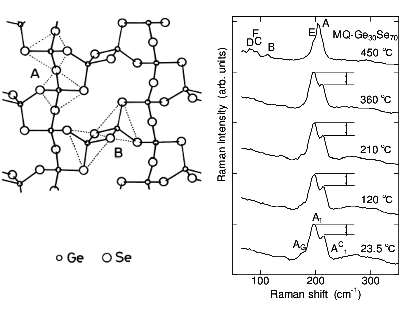
After he graduated Osaka City University, he changed his research laboratory in order to extend the scientific viewpoint as a young researcher. He was in Department of Physics, Graduate School of Science, Osaka University with a master's (MA) degree in Physics. Master thesis: Raman scattering spectroscopy of thermal/photo-induced structural changes in non-crystalline GeSe2 prepared by vacuum-evaporation and melt-quench methods
As a member of the Laboratory of Prof. Murase (*) , he investigated the optical and thermal properties of non-crystalline GeSe2, one of chalcogenide semiconductors. Some of digital versatile discs (DVDs) utilize amorphous-crystal phase transitions by laser-irradiation annealing. The crystallization mechanisms were, however, not fully elucidated. Accordingly, he focused his interest on the elucidation of the above-mentioned phase transition mechanism from the aspect of physics. Before the graduation, he wrote his first "first-authored" paper. The paper has a small impact at that time; however, the fact "Writing a paper by himself" strongly influence his future, though he was not aware of the impact on his life.
(*Murase Lab was closed after the retire of Prof. Murase.)
Phase 3|Apr. 1997 to Mar. 1999: ROHM CO. Ltd.,
![]()
After the graduation of Graduate School of Osaka University, he decided to work at the LSI division since he wanted the industrial viewpoint on semiconductors. Without any connection, he entered ROHM Co. Ltd., He was in charge of the LASER-trimming technology and the trial products of LSIs.
He really enjoyed the day in ROHM with the members of the LSI division. Here, he would like to express a word of appreciation. C. Yoshida, she is the most reliable of all assistants whom I have been working with. Her kindness and correct work were very helpful. He is also grateful to the manager, Fuwa, the vice-manager, Matsumoto, the section chief, Ohmori, Sawase, Hashimoto, and the friends, Ohta, Shimizu, Hirano, Yamazaki.... for their kindness and helpful advices.
After two-years work experience at ROHM, he desired to step up his carrier not only in the technology field but also in the science field. At that time, the acquisition of Ph D. degree seemed to be the best of all choices because it is a kind of a "passport" as an engineer. Needless to say, the process of the Ph D. degree acquisition provides the information that turns out to be intelligence. It is also a chance for extending the viewpoints through the discussion with various researchers. Accordingly, he made up his mind and left ROHM Co. Ltd., in March 1999. What is called a kind of "Datsu-Sala", which is one of the famous word of Japanese language meaning the voluntary resignation to get another carrier and/or chance.
Phase 4 - 1|Apr. 1999 to Mar. 2002: Osaka City University (2nd term).
![]()
After the retirement of ROHM CO. Ltd., he was with Department of Applied Physics, Graduate School of Engineering, Osaka City University for his main purpose: the acquisition of a Ph. D's degree in Engineering.
Ph. D thesis : Ultrafast spectroscopy of coherent phonons in semiconductor superlattices
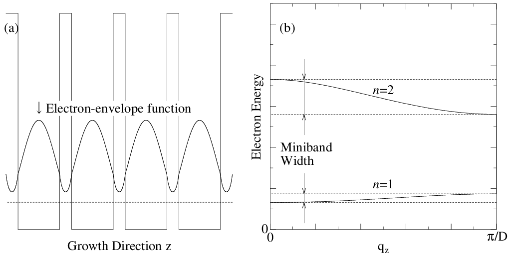
He studied at the Laboratory of the Optical Properties and Functions of Materials as a graduate student in doctoral program. Here, I studied various (!) optical properties of semiconductor heterostructures including quantum wells ( QWs ) and superlattices ( SLs ). His research activities were focused on the following three themes:
- Control of the Wavefunctions in Semiconductor Superlattices by Electric Fields.
- Coherent Terahertz Phenomena with a Femtosecond-Pulse LASER
- Photoreflectance Spectroscopy of Semiconductor Heterostructures.
"Control of the Wavefunctions in Semiconductor Superlattices by Electric Fields" is related to not only interband transitions but also intersubband transitions in SLs and QWs. "Interband transition" means the transitions between the conduction ( electron ) and valence ( hole ) bands. In contrast, "Intersubband transition" is the transition between the quantized levels within the conduction or valence band. Quantum cascade lasers ( QCLs ) and quantum well infrared photodetectors ( QWIPs ), which are key devices for mid-infrared ( 4 mm to sub-mm ) spectroscopy, utilizes this intersubband transition phenomena. At that time, the door for terahertz spectroscopy begun to open.
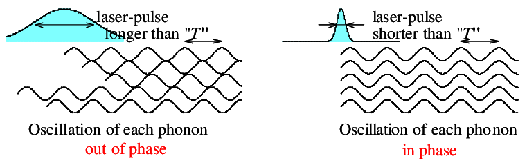
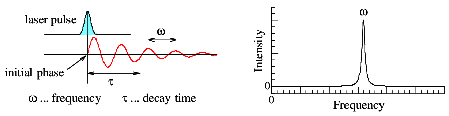
"Coherent Terahertz-range Phenomena with pump-and-probe technology: Ultrafast Phenomena brought by Progress in Femtosecond-Pulse laser systems" includes the coherent phonons that are an in-phase oscillatory phenomena excited by the irradiation of ultrashort laser pulses. Progress in femtosecond pulse laser technologies enables to observe oscillatory profiles of coherent phonons: the oscillatory profiles can be recorded as a function of time delay between the pump and probe laser pulses. This implies that we can measure phonon signals in the time domain. From the time-domain signal of coherent phonons, we can obtain information on the initial phase and decay time, which conventional cw-Raman spectroscopy do not provide.
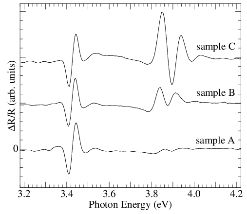
"Photoreflectance Spectroscopy of Semiconductor Heterostructures" has important roles on the evaluation of transition energies and surface/interface electric field strength of semiconductors. Its progress is a key for the developments of semiconductor heterostructure devices that includes heterojunction bipolar transistors (HBTs) and high electron mobility transistors (HEMTs).
Fortunately, his research activities went quite well. Among them, the research on the theme ( II ) became the most successful. Consequently, he has succeeded in acheving the Ph. D's degree of engineering in March 25, 2002. The title of Ph.D thesis is "Ultrafast Spectroscopy of Coherent Phonons in Semiconductor Superlattices" (Degree Number: 1933). His Ph.D thesis, which was written in Japanese, is available in this site ( Click here, and jump to the down-load site ).
Phase 4 - 2|Apr. 1999 to Mar. 2002: Adjunct Lecturer at Osaka Institute of Technology
![]()
During the doctor-course student, he worked at Osaka Institute of Technology as an adjunct lecturer of the experimental-physics course. The above-mentioned experience leads to his present job, though, at that time, he was not aware of the importunateness of this experience on his future activities.
Phase 5|Apr. 2002 to Feb. 15, 2008: Mitsubishi Electric Corporation.
Mitsubishi Electric Corporation
![]()
In 2002, he joined Mitsubishi Electric Corporation , Hyogo, Japan, where he had been engaged in the research and development of the characterization and design technologies of epitaxial structures of HBTs and HEMTs. He researched on "Photoreflectance spectroscopy of semiconductor heterostructure devices" for a high-performance characterization method of epitaxial wafers. In addition, he collaborated with epiwafer venders to improve quality of AlGaN/GaN epitaxial wafers.
Phase 6|Apr. 2008 to March 2013: The University of Shiga Prefecture
Department of Electronic Systems Engineering.
The University of Shiga Prefecture
![]()
In the beginning of 2008, he made a restart in his life. The about six-year experience was not enough to fulfill his life. He decided to move from Mitsubishi Electric Corp., -- the world of engineers --, to The University of Shiga Prefecture , -- the world of scientists --. He is working with Department of Electronic Systems Engineering as an associate professor. At present, since our department is under the establishing process, he carries out various experiments using facilities of other universities. In his research activity at The University of Shiga Prefecture, he would like to investigate or quest the issues of condensed matter physics left behind the state-of-the-art technologies and to contribute the both the fields of engineering and science.
Phase 7|Apr. 2013 to Present: Osaka City University
Department of Applied Physics, Graduate School of Engineering.(3rd term)
![]()
In the beginning of 2013, he moved to Osaka City University. This is a third time for him. He has been working as an associate professor. At present, he has various chances to develop his ability. He always enjoys and feels a swingy research. He copes with phenomina of cutting-edge terahertz spectroscopy. He also engages GaN-based novel materials. He struggles with the research lab. style because the passed time makes the considerable change in the Lab. Now, he tries to establish his new style for the rearch avtivities, and, at the same time, he enjoys it.
Phase 8|Apr. 2017 to Present: Sophia Unversity (Concurrent position)
Faculty of Science and Technology
![]()
Since Apirl, 2022, he has been a Collaborative Reseacher with Nakaoka LAb. at Faculty of Science and Technology. He is engaged in terahertz time-domein spectroscopy of GaAa surface treated with the use of fast atom bonbardment.
Phase 9-1|Apr. 2022 to Present: Osaka Metropolitan University at Sugimoto Campus
Division of Physics and Electronics, Graduate School of Engineering.
![]()
In April 2022, Osaka Prefecture University and Osaka City University united to form the Osaka Metropolitan University. Accordingly, since 2022, he has been an Associate Professor with Division of Physics and Electronics, Graduate School of Engineering, Osaka Metropolitan University. We are planned to move Osaka Meropolitan UNivesity at Nakamozu (Sakai) Campus in April 2024.
Affiliation Society
The Physical Society of Japan (JPS).
The Japan Society of Applied Physics (JSAP).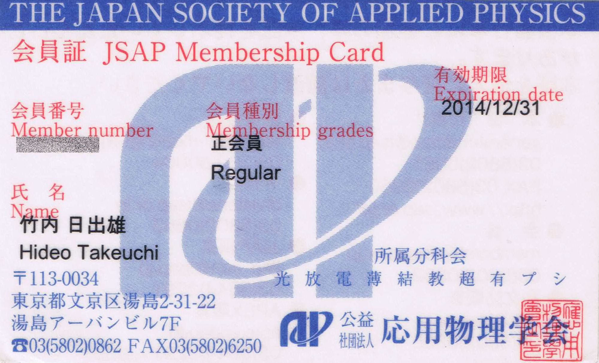

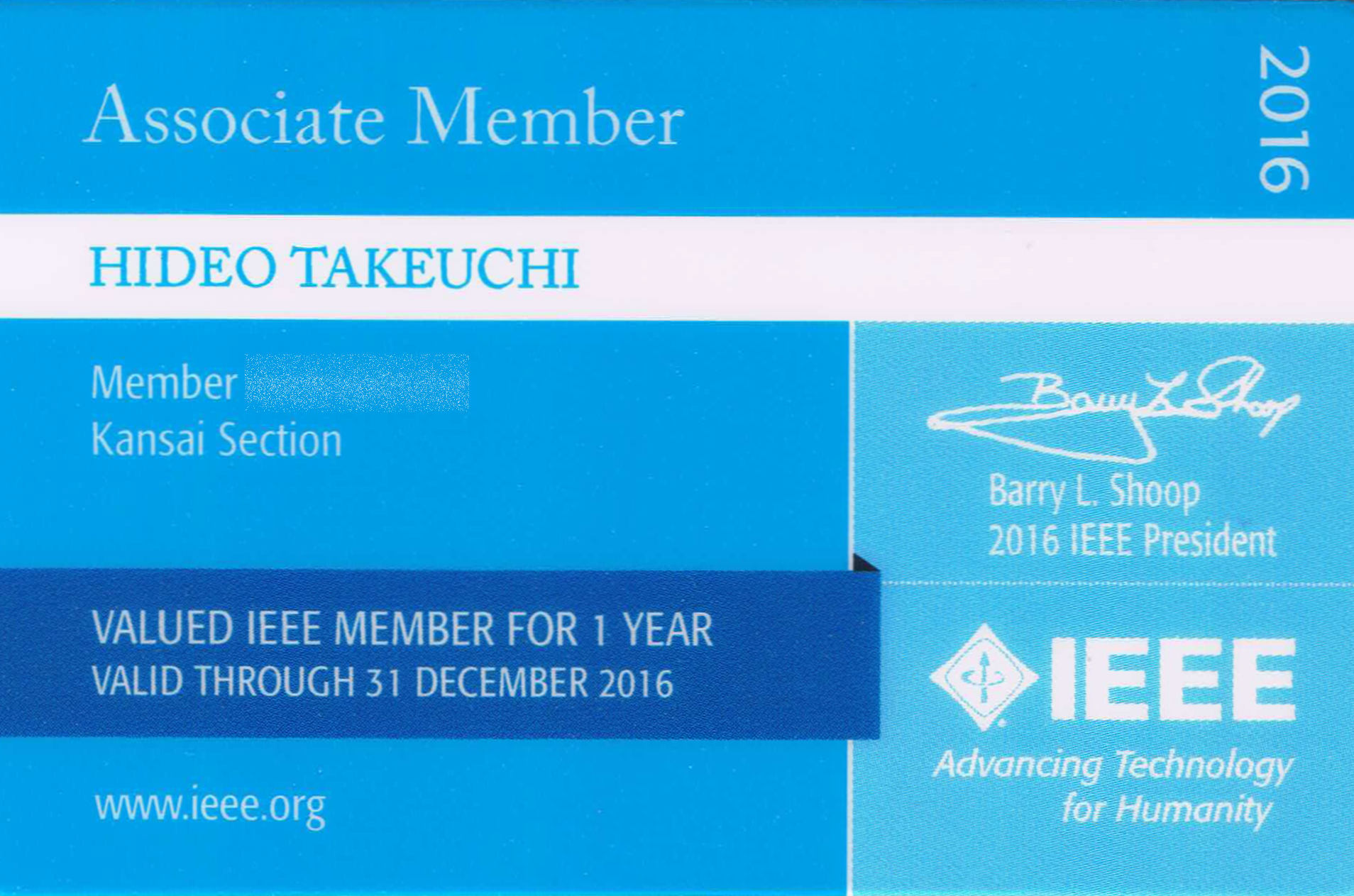
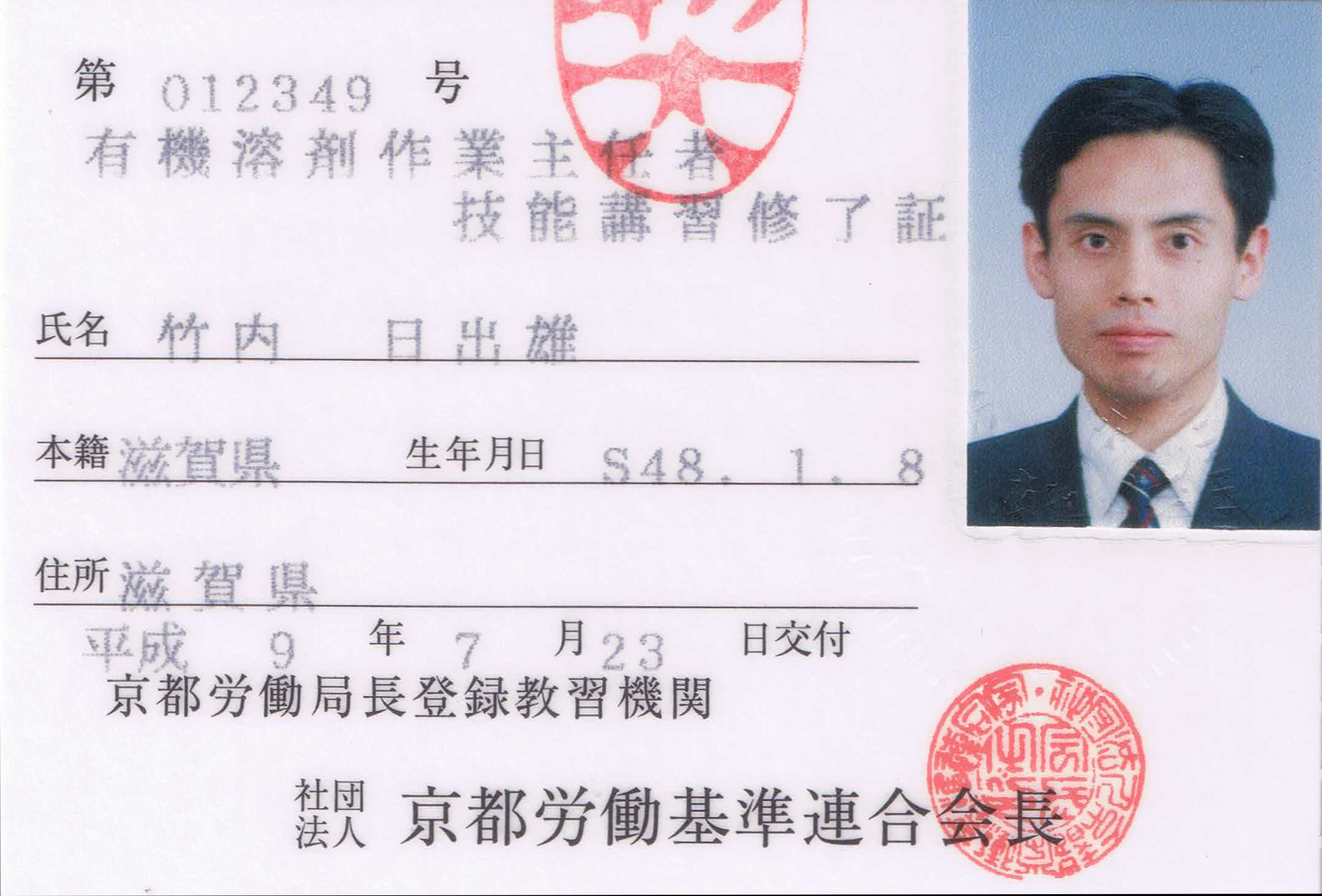
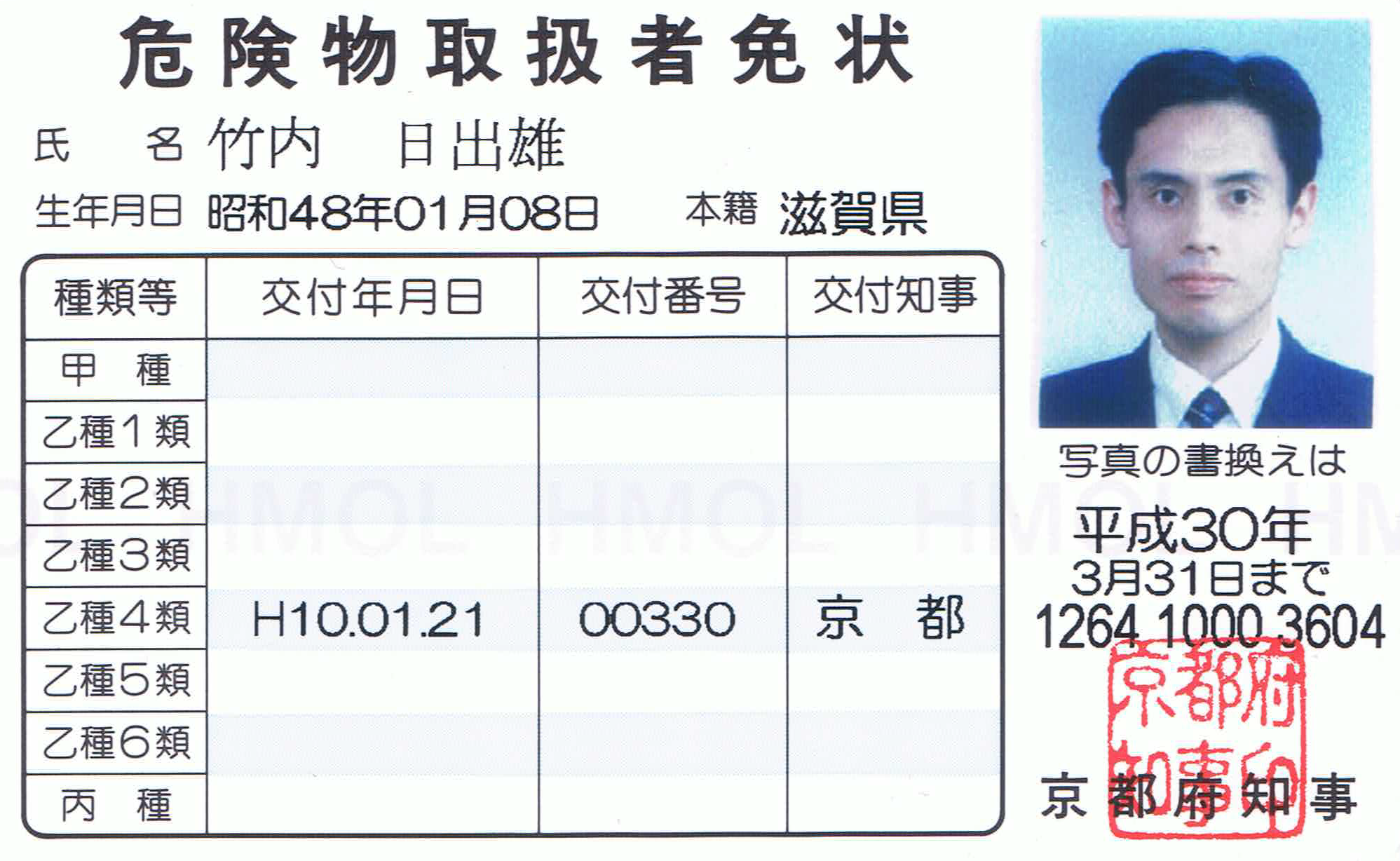
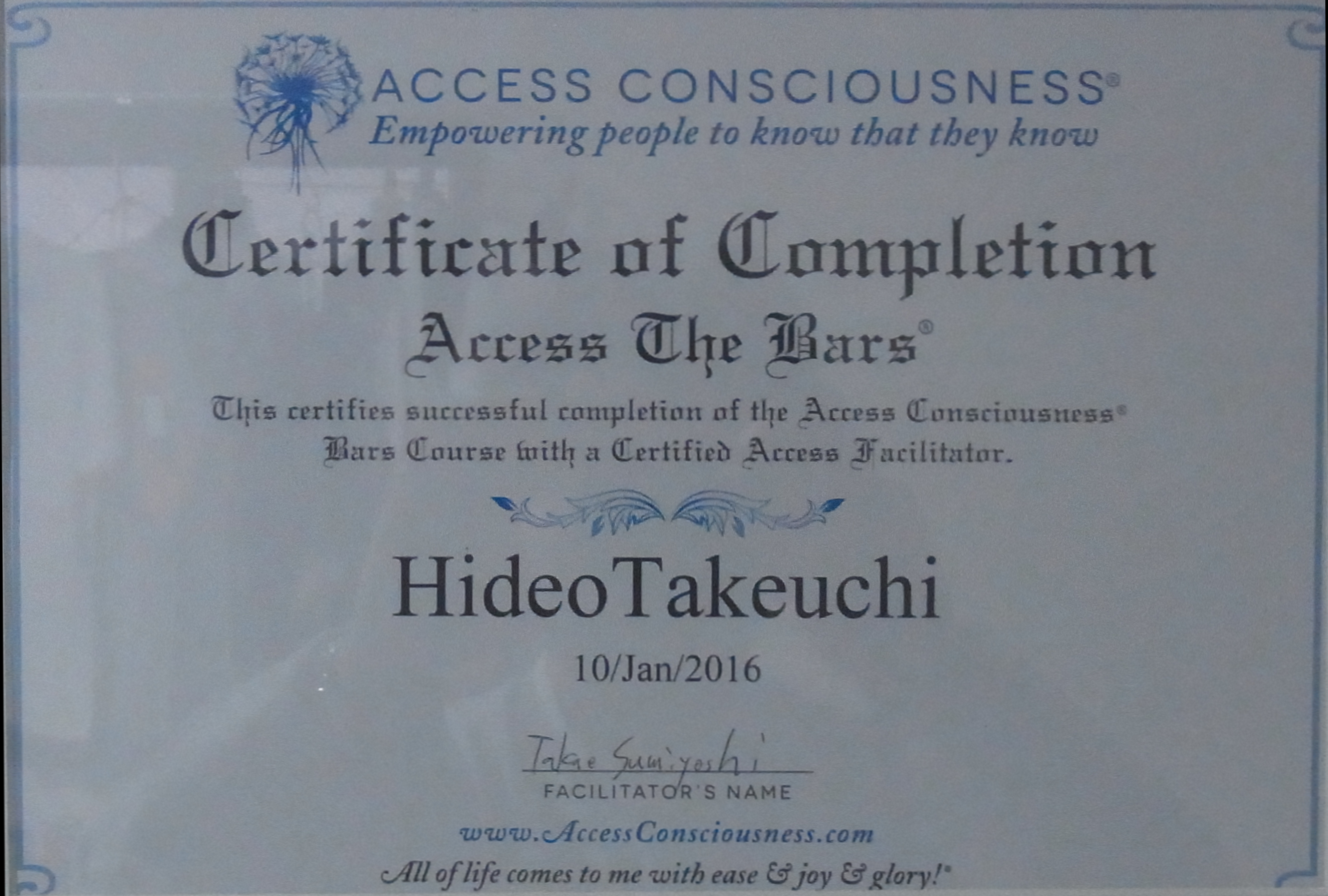
License
Organic solvent work chief (Domestic, effective in Japan).
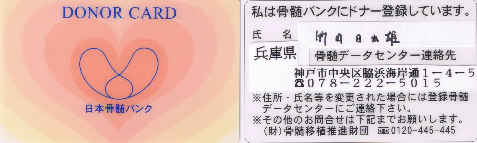
Donor Cards (Effective in Japan)
Bone-marrow bank card.

... and so on
My way of life
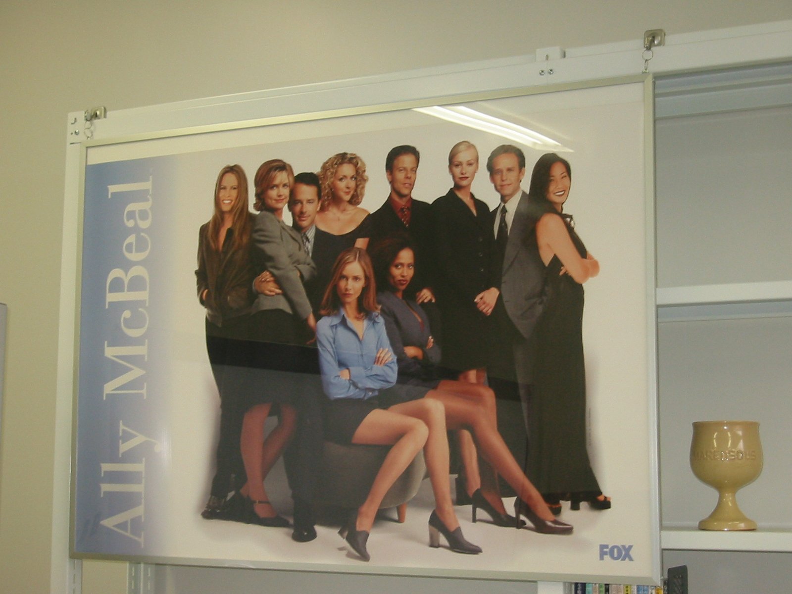
The real truth is I probably don't want to be too happy or content. Because ... then what? I actually like the quest, the search. That's the fun. The more lost you are, the more you have to look forward to. What do you know? I'm having a great time, and I don't even know it.-- Ally McBeal, season 1, episode 1 "Pilot", ( FOX TV, September 8, 1997 ).
My favorites:
- Starbucks Caffe Mocha
- Jazz: Ms. Chihiro Yamanaka, Mr. Oscar Peterson, Bil Evance, Stan Gets ...
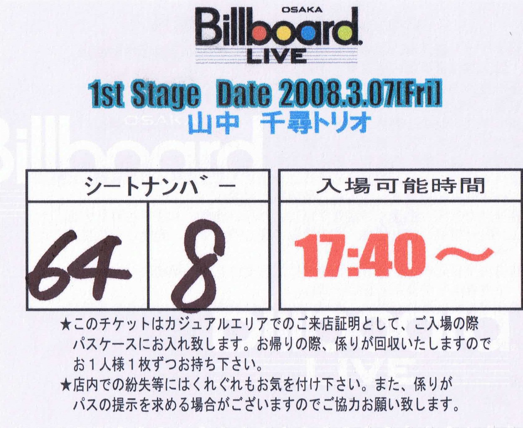
- Ally-McBeal Show
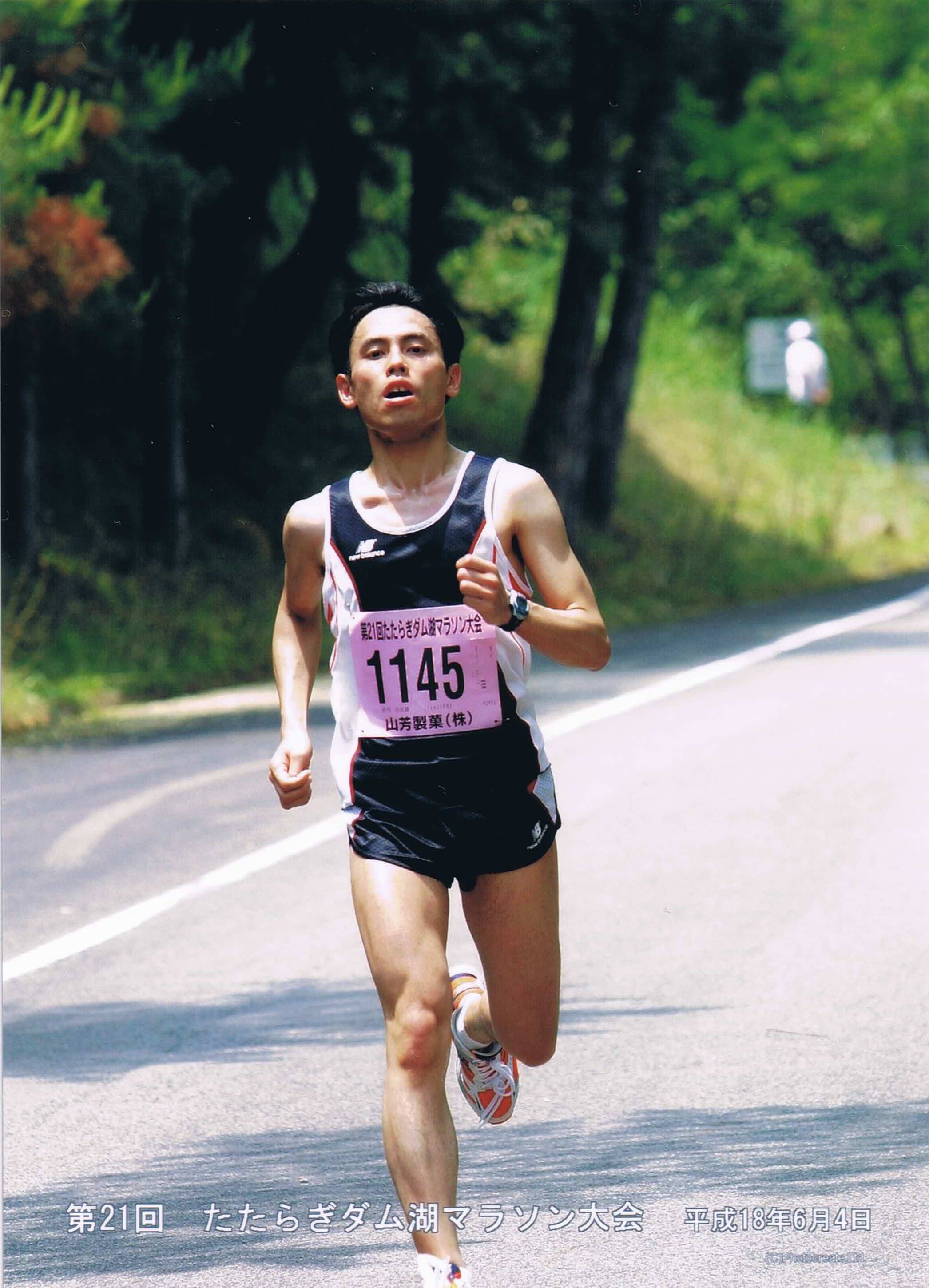
- Running:
Fastest time 19:28 at 18th Kobe city marathon (Jan. 28, 2008); 10 km, 40:04 at 30th Suigo-no-Sato marathon (Nov. 6, 2006).
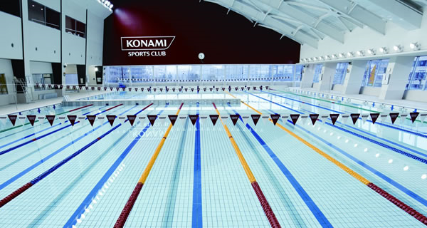
- Swimming: 3~4 hours swim in Sunday or Saturday.
Freestyle (50 m) about 35 sec, in usual.
My treasure
His best treasure is the following word given by his friend, Ms. Y.Y., who shares various experiences each other.
"Takeuchi-kun excellently hides and shows his Ph.D. degree at the same time."
His facebook page reflects his hobbies and interest. He can express himself more frankly by this way than by writing lots about me by himself, he thinks.
Thank you for your attention.