Home![]() Research description
Research description![]() Theme IV
Theme IV
Research description
Theme IV. Terahertz time-domain spectroscopy A: Emission from surge currents of photogenerated carriers
Teraherts electromagnetic waves from the photogenerated carrier surge current induced by the illumination of the femtosecond laser at the semiconductors surface
1 : Summary of outline, objectives and outcomes
Viewgraphs (in English) ... see the presentation materials
Terahertz electromagnetic waves have a frequency range between infrared light and microwave. Terahertz spectroscopy is sometimes called cutting-edge spectroscopy. Resent progress in terahertz spectroscopy stimulates research and deveplopment of intense terahertz electromagnetic wave emitters. The application of terahertz wave has a full of variety. For example, Hu and Nuss observed the terahertz transmittance images of the two leaves: freshly cut leaf and the same leaf after 48 hours [B. B. Hu and M. C. Nuss, Opt. Lett. 20 (1995) 1716]. They demonstrated the freshness between the two leaves can be clearly evaluated from the terahertz transmittance images. Terahertz waves are sensitive to explosive chemical materials. Accordingly, the terahertz waves are applicable to a security system in airports because conventional x-ray inspection systems are insensitive to chemical materials. The above-mentioned characteristics of the terahertz wave lead to the reason why terahertz-wave spectroscopy is attractive. The terahertz waves are useful to investigate the vibration of biological molecules, dielectric constant of materials, and so on. This is the reason why terahertz spectroscopy is attractive.
The progress of terahertz spectroscopy is brought by the development of the femotosecond pulse laser system. Here are the femtosecond pulse laser system (Fig. 1) and the experimental setup for terahertz spectoroscopy.
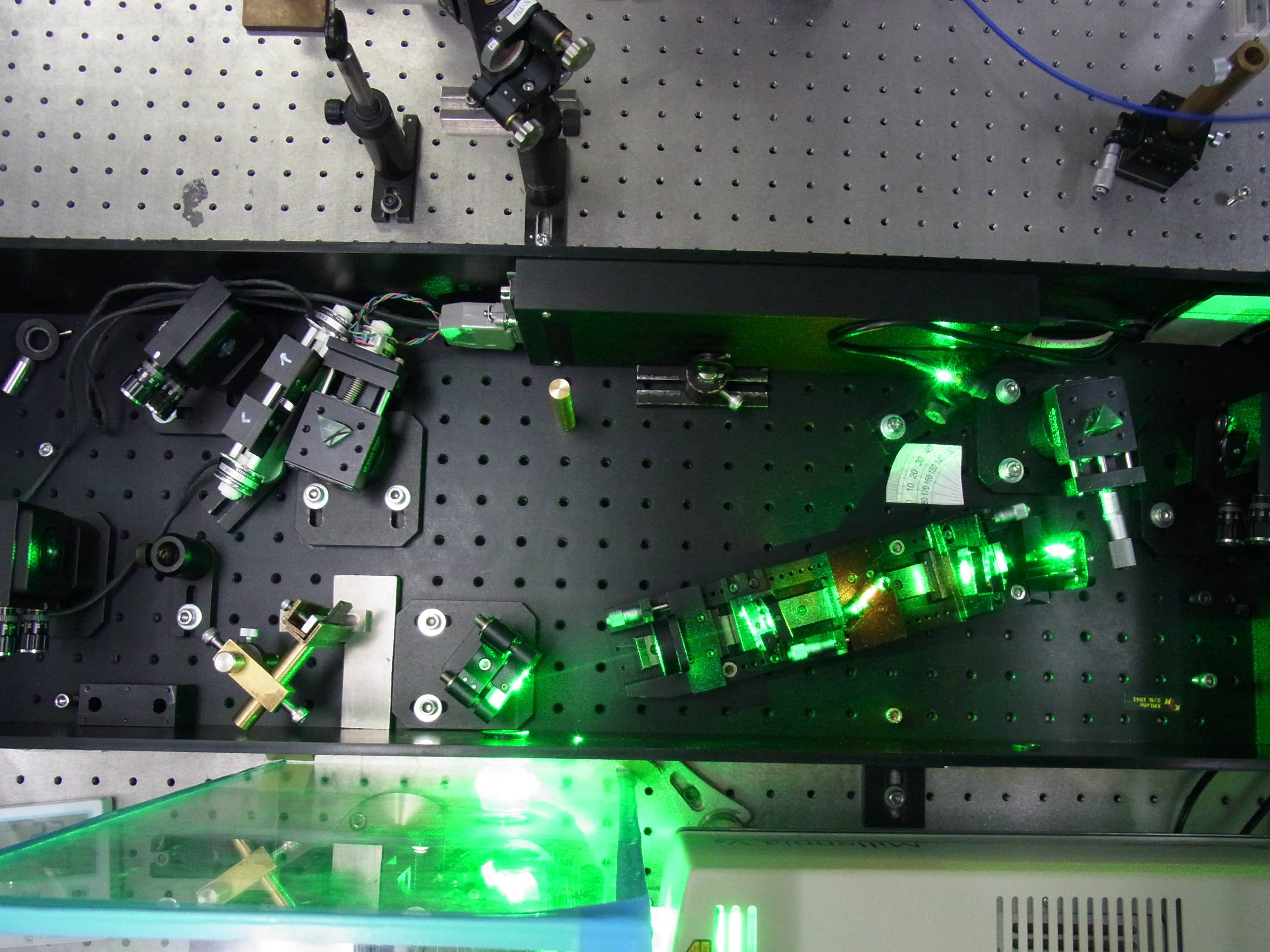
Figure 1: Examples of a femtosecond pulse laser system. (ex.) Kaptain and Milleniar.
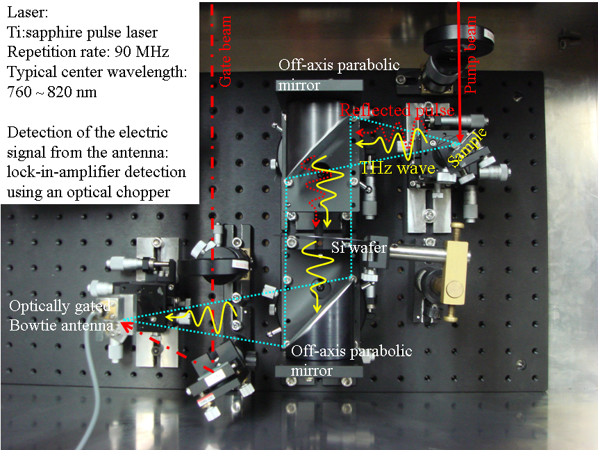
Figre 2: Example of an experimental setup for terahertz spectroscpy.
In advance to the detaled explanation of the description of the our attention and strategy, we introduce an example of the terahertz spectroscopic measurement systems. The following method is the so-called optical gating. The time-domain terahertz-wave signals from the samples are measured with use of laser pulses with a duration time less than 100 fs. The measurement system for the terahertz wave is shown in Fig. 2 as a photograph. The sample, which is illuminated by the pump beam, emits a terahertz wave along the reflection direction of the pump beam. The emitted terahertz wave was collected with use of two off-axis parabolic mirrors. The high resistivity silicon wafer was placed as a filter for the pump beam. The collected terahertz wave was focused on the photoconductive antenna with a gap of several um order formed on a low-temperature-grown GaAs. The photoconductive antenna was optically gated with use of the laser-pulse beam (gate beam), which was controlled by the mechanical delay line, the so-called stepper. Consequently, the terahertz wave was detected only in the case where the antenna was illuminated by the gate beam. The above-mentioned method for the detection of the terahertz wave is the optically gating technique (Nuss & Orenstein, 1999; Bolivar, 1999)
Most of the terahertz-wave measurement systems equip with a photoconductive antenna as a terahertz emitter. Figures 3(a) and 3(b) show a typical bow-tie antenna and dipole antenna, respectively. The metal electrodes of the antennas are formed on the low-temperature-grown GaAs epitaxial layer. The gap of the antenna is of the order of um. The generation mechanism of the terahertz wave is schematically shown in Fig. 4. The illumination of the laser pulses (the pump beam) induces the surge current of the photogenerated carriers J. According to Faraday’s law of induction, the electric field of the terahertz wave ETHz(t) is expressed by the time delivative of the surge current.
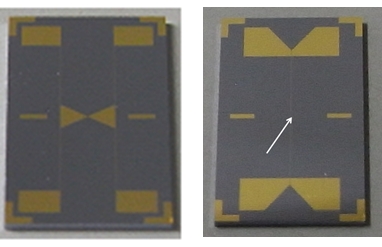
Figure 3: Typical photoconductive attenas. (left) Bow-tie anntena. (right) dipole anntea.
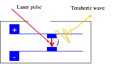
Figure 4: Schematics of the terahertz emission from the photoconductive attenas.
Compound semiconductors with a surface electric field, by being irradiated by fs-laser pulses, emit the terahertz wave originating from a surge current flowing in the surface depletion layer. This phenomenon provides us a convenient terahertz emitter free from a device fabrication for an external applied bias. In the above terahertz emission mechanism, the doping concentration is a major factor determining the depletion-layer width and surface electric field, which are in the relation of tradeoff on the doping concentration. In order to obtain intense terahertz emission, earlier works focused on searching a proper compound semiconductor and subsequently adjusted the doping concentration. Moreover, external magnetic fields, which are of the order of 1 T, were used for enhancing the terahertz emission; however, the terahertz spectroscopic system with use of the magnetic field generator lacks the advantage of being convenient.
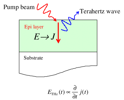
Figure 5: Schematics of the terahertz emission from the surface of the compound semiconductors.
In the first stage of Theme IV, we have explored the feasibility of enhancing the terahertz emission intensity by appropriately designing an epitaxial layer structure. We proposed an undoped GaAs (i-GaAs)/n-type GaAs (n-GaAs) epitaxial layer structure as a feasible intense terahertz emitter. This structure has two features. First, in the i-GaAs(200 nm)/n-GaAs(3um 3x1018cm-3) structure has an upward surface band bending. The electric field is estimated to be 35 kV/cm, which is sufficient to cause a drift motion of carriers. Accordingly, the photogenerated electrons flow to the inside of the crystal. The second feature is a relatively thick depletion layer. The whole i-GaAs layer is depleted, so that the free carrier absorption is suppressed at the surface. We demonstrated that the i-GaAs/ n-GaAs structure is effective to enhance terahertz emission and that the emission intensity from the i-GaAs/n-GaAs sample can exceed the emission intensity from i-InAs that is known as one of the most intense terahertz emitters.
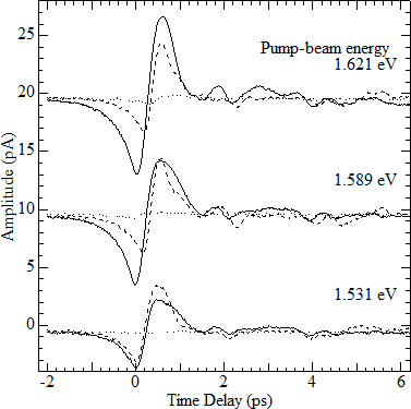
Figure 6: Amplitude of the terahertz waveform as a function of time delay at room temperature. The solid, dotted, and dashed lines indicate the time domain signals of the i-GaAs/n-GaAs, n-GaAs, and i-InAs samples. The pump-beam power was 20 mW, while the pump-beam energies were 1.531, 1.589, and 1.621 eV.
In the research field of terahertz waves, most of the efforts have been focused on how to enhance the terahertz intensity of emitters or on how to obtain the good terahertz images, which indicates that the terahertz wave has been attracting much attention as a probing tool. The terahertz waves contain a lot of information on physics of the source material. We focused our attention on this viewpoint and investigated the direction of the surface potential bending using terahertz wave measurements. We utilized the polarity of the terahertz wave. We have investigated the polarity of the terahertz wave from GaAs-based dilute nitride (GaAs1-xNx and InyGa1-yAs1-xNx) epitaxial layers in order to clarify the effects of nitrogen incorporation on the direction of the surface band bending, using the i-GaAs/n-GaAs epitaxial layer structure and a semi-insulating GaAs (SI-GaAs) crystal as reference samples. The i-GaAs/n-GaAs sample has au upward band bending at the surface region, which indicates that photogenerated electrons flow into the inside. In the measurement of the terahertz wave, it is observed that the polarity of the terahertz wave from the SI-GaAs crystal is the same as that of the i-GaAs/n-GaAs; namely, the present SI-GaAs crystal has an upward band bending. In contrast, the terahertz-wave polarity is reversed in the GaAs1-xNx sample with x = 1.53 %; namely, the GaAs1-xNx sample has a downward band bending. The terahertz-wave polarity reversal is attributed to the phenomena that the conduction band bottom is considerably lowered by the band anticrossing peculiar to GaAs1-xNx, which results in approaching the conduction band bottom to the surface Fermi level. This modifies the direction of the surface band bending connected with the polarity of the terahertz wave. We have also investigated terahertz wave from an InyGa1-yAs1-xNx epitaxial layer (x = 5.0 %, y = 14 %). It has been found that the terahertz-wave polarity is also reversed in the InyGa1-yAs1-xNx sample. Thus, we conclude that the direction reversal of the surface potential bending induced by the band anticrossing is universal in GaAs-based dilute nitrides. Here, I would like to emphasis that the terahertz wave, the "small" energy phenomenon, provides a "large amount" of the information on the ultrafast carrier dynamics, surface potential structures, and physics of the terahertz-wave-emitting materials.
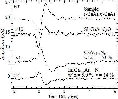
Figure 7: Amplitudes of the terahertz waveforms of the i-GaAs(200 nm)/n-GaAs(3.0 um, 3x10^18 cm-3), semi-insulating GaAs, and GaAs1-xNx (x = 1.53%) and InyGa1-yAs1-xNx (x = 5.0%, y = 14%) samples as a function of time delay at room temperature. Pump-beam power: 40 mW; Wavelengths of the pump beam: 800 nm. For clarity, each waveform is vertically shifted.
We note that the combination of the terahertz spectroscopic analysis and photoreflectance measurements is effective to quantitatively investigate the surface potential structure of GaAs1-xNx epitaxial layers. Figures 8(a) and 8(b) show the terahertz waveform and photoreflectance spectrum of the GaAs1-xNx epitaxial layer with x = 0.43%. From the oscillation patterns in photoreflectance spectrum, the Franz-Keldysh oscillation is a measure of the surface electric field "strength", while the terahertz waveform gives a information on the "direction" of the electric field; namely, the combination of the terahertz spectroscopic analysis and photoreflectance measurements leads to the detailed analysis of the surface electric field.
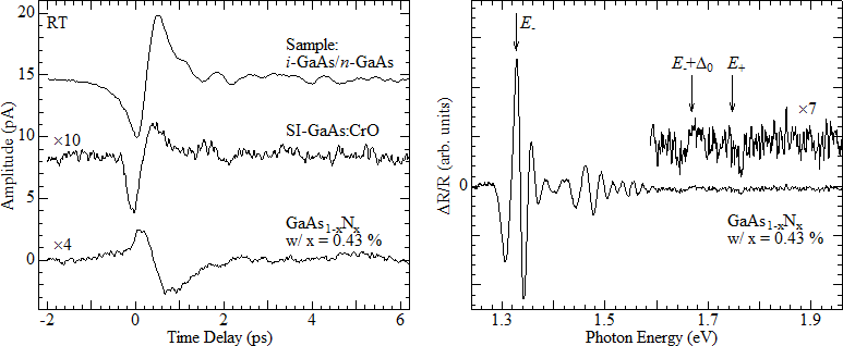
Figure 8: (from left) (a) Amplitudes of the terahertz waveforms of the i-GaAs(200 nm)/n-GaAs(3.0 um, 3x10^18 cm-3), semi-insulating GaAs, and GaAs1-xNx (x = 1.53%) and InyGa1-yAs1-xNx (x = 0.43%) samples as a function of time delay at room temperature. (b) Photoreflectance spectrum of the GaAs1-xNx sample at room temperature. The oscillation patterns, which ranges from 1.4 to 1.6 eV, are the so-called Franz-Keldysh oscillations.
The research activities on terahertz waves/terahertz spectroscopy brought the following ** papers.
2 : List of outcomes
_Publications
1 "Enhancement of terahertz electromagnetic wave emission from an undoped GaAs/n-type GaAs epitaxial layer structure".H. Takeuchi, J. Yanagisawa, T. Hasegawa, and M. Nakayama.
Applied Physics Letters vol. 93, 081916 (2008).
# Link to the online-journal site
2 "Effects of nitrogen incorporation on a direction of a surface band bending investigated by polarity of terahertz electromagnetic waves in GaAs1-xNx epitaxial layers".
H. Takeuchi, J. Yanagisawa, J. Hashimoto, and M. Nakayama.
Journal of Applied Physics vol.105, 093539 (2009).
# Link to the online-journal site
3 "Intense emission of terahertz electromagnetic wave from an undoped GaAs/n -type GaAs epitaxial layer structure".
H. Takeuchi, J. Yanagisawa, T. Hasegawa, and M. Nakayama.
Physica Status Solidi (c) vol.6, pp.1513-1516 (2009).
-Proceedings of the 35th International Symposium on Compound Semiconductors, Rust, Germany (2008).
# Link to the online-journal site
3 : Posters and viewgraphs
1 "Intense emission of terahertz electromagnetic wave from an undoped GaAs/n-type GaAs epitaxial layer structur".
H. Takeuchi, J. Yanagisawa, T. Hasegawa, and M. Nakayama.
The 35th International Symposium on Compound Semiconductors (ICSC2008) September 21-24, 2008, Europa-Park, Rust, Germany.
*** Poster Presentation P34 (September 23, Tuesday) ***
The abstract is here. The poster is here.
2 "Direction reversal of the surface band bending in GaAs-based dilute ni-tride epitaxial layers investigated by polarity of terahertz electromagnetic waves".
Hideo Takeuchi, Junichi Yanagisawa, and Masaaki Nakayama.
The 14th International Conference on Narrow Gap Semiconductors and Systems (NGSS-14) July 13-17, 2009, Sendai, Japan.
*** Oral Presentation: Talk-8 (July 15, Wednesday) ****
The abstract is here. The viewgraph is here.