Home![]() Research description
Research description![]() Theme III
Theme III
Research description
Theme III. Photoreflectance spectroscopy
Characterization of epitaxial layer structures using photoreflectance spectroscopy: analysis of semiconductor device epitaxial wafers and assessment of device fabrication photoreflectanceocesses
1 : Summary of outline, objectives and outcomes
Viewgraphs (in English) ... see the photoreflectanceesentation materials
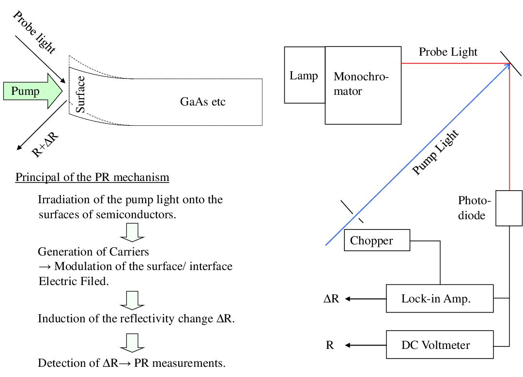
Modulation spectroscopic measurements probe the changes in optical constants caused by applying modulations (electric field, stress) to samples. Photoreflectance techniques are also included in modulation spectroscopy: it detects the reflectance change caused by intermittent irradiation of a pump beam. This modulate the built-in electric field owing the carriers generated by the pump beam. Since the mechanism of photoreflectance relies only on the light illumination, the photoreflectance measurement has advantages of being non-destructive and contactless. Figure 1 shows the schematics of the photoreflectane mechanisim and experimentat setup. The experimental system is quite simple.
Photoreflectance spectra usually exhibit oscillatory patterns, the so-called Franz-Keldysh oscillations. This phenomena connect with the presence of the internal electric field and/or surface electric field resulting from the surface Fermi level pinning. The Franz-Keldysh oscillations are, therefore, applicable to evaluate the electric fields and electrostatic potential structures. Moreover, it has been attracting much attention for the application to monitor the characteristics of semiconductor surface during the device fabrication photoreflectanceocess. The physics of the photoreflectance and Franz-Keldysh oscillations in bulk crystals were intensivelyinvestigated in 1960's and 70's. In contrast, the characteristics peculiar to the heterostructures have hardly been taken into account. As a result, the Franz-Keldysh oscillations of heterostructures had been analyzed using the models and theories for bulk crystals. To settle this issue, taking account of the interference effects, which originating from layered structures, I derived the calculational model on the Franz-Keldysh oscillations profile, which revealed that the phase of the Franz-Keldysh oscillations is mainly influenced by the interference effect. I demostrated that the calculational model is effective to photoreflectance precisely estimate the built-in electric field and optical transition energy. In addition, I found that the Franz-Keldysh oscillations in a certain heterostructure is identified through the analysis of the phase of the Franz-Keldysh oscillations.
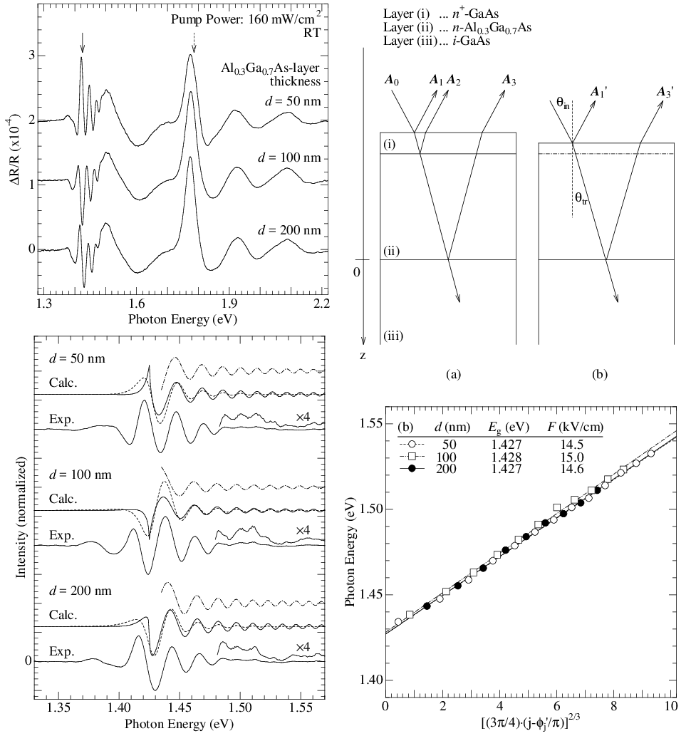
Photoreflectance spectra of the n+-GaAs/n-Al0.3Ga0.7As(d nm)/i-GaAs heterostructures with d = 50, 100 and 200 nm. The profile of each photoreflectance spectrum considerably differs in the photon-eneggy range from 1.4 to 1.7 eV. Schematic diagram of the reflected probe light from an n+-GaAs/n-Al0.3Ga0.7As(d nm)/i-GaAs heterostructure. A0 is the incident light. A1, A2, and A3 are the probe light reflected at the surface of the n+-GaAs cap layer, the probe light reflected at the n
In general, the photoreflectance spectra depend on the intensity of the photoreflectanceobe beam since it steadily illuminates samples during the measurement and hence the generated carriers screen the electric field. In the conventional photoreflectance measurements for estimating the internal/surface electric fields, the photoreflectance probe-beam intensity is suppressed to remove the screening effects. This makes the signal detection difficult. I pproposed a novel substituting method from the viewpoint of positively utilizing the screening effects. The numerical calculations elucidated that, at the steady illumination, the surface electric fields are strongly influenced by the two parameters characteristic of the surface, the surface Fermi level and surface recombination velocity. The surface recombination velocity corresponds to the recombination lifetime at the surface. The calculational results indicate that the surface Femi level and surface recombination velocity are estimated through the following procedure. In the first stage, the surface electric field is estimated from the Franz-Keldysh oscillations and is plotted as a function of probe-beam power density. Next, the surface electric field is calculated on the basis of the Schrodinger-Poisson equation and is fitted to the experimentally estimated surface electric field using various sets of the above-mentioned two surface parameters. As a result, the two surface parameters are derived. I varifyed my strategy, using an undoped GaAs/n-type GaAs structure, that the two surface parameters are estimated through the above procedure.
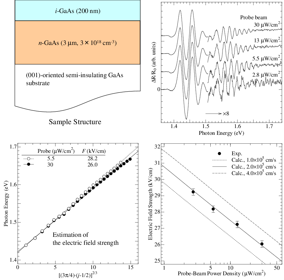
Sample structure. Photoreflectance spectra at various probe-beam power densities at room temperature. The pump-beam power density used is 80 mW/cm2. Linear plot of the extrema of the Franz-Keldysh oscillations . The closed and open circles indicate the linear plots of the extrema of Franz-Keldysh oscillations in the photoreflectance spectra measured at the probe-beam power densities of 30 and 5.5 μW/cm2, respectively. Comparison between the calculated and estimated surface electric field strengths with respect to the probe-beam power density. The closed circles indicate the surface electric field strengths estimated from the Franz-Keldysh oscillations. The dashed, solid, and dashed-and-solid curves indicate the surface electric field strengths calculated at the surface Fermi level of ±0.0 eV. The values of the surface recombination velocity employed are as follows: 1.0x105 cm/s for the dashed curve, 2.0x105 cm/s for the solid curve, and 4.0x10>5 cm/s for the dashed-and-dotted curve. *: The details, see Takeuchi et. al Journal of Applied Physics vol.97, 063708 1-16 (2005).
In addition, the effects of the nitridation of the GaAs surface were characterized by the two surface parameters. I clarifyed that the surface nitridation causes the considerable change in the energy level of the surface Fermi pinning.
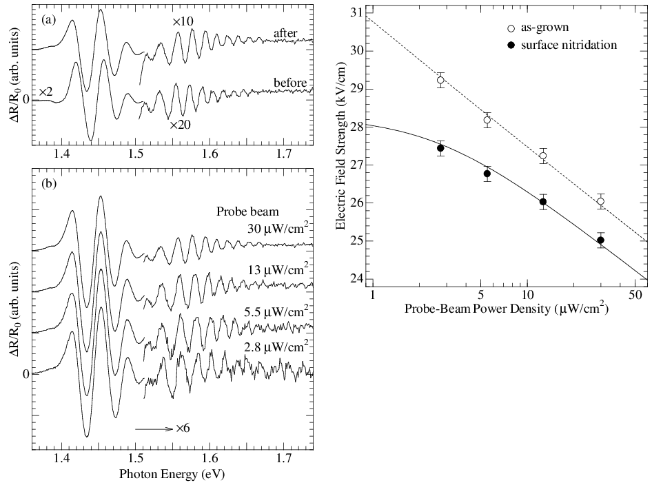
Photoreflectance spectra from the i-GaAs(200 nm)/n-GaAs(3.0 μm, 3x1018 cm-3) before and after the surface nitridation measured at the probe-beam power density of 30 &muW/cm2. Photoreflectance spectra after the surface nitridation measured at various probe-beam power densities. Comparison between the calculated and estimated surface electric field strengths with respect to the probe-beam power density. Closed circles: surface electric field strengths estimated from the Franz-Keldysh ocsillations after the surface nitridation. Open circles: re-plotted surface electric field strengths of the as-grown i-GaAs/n-GaAs structure. Dashed curve: calculated surface electric field strength using the surface Fermi level of ±0.0 eV and surface recombination velocity of 2.0x105 cm/s. Solid curve: calculated surface electric field strength using the surface Fermi level of +0.13 eV and surface recombination velocity of 1.0x105 cm/s. It is clear that the surface Fermi level is shifted to the conduction band. (*) The details, see Takeuchi et. al, Journal of Applied Physics vol.97, 063708 1-16 (2005).
The photoreflectance measurements are useful to assess III-nitride heterostructures, the potential structure of which depends on spontaneous polarization and piezoelectric polarization. The potential structures are usually evaluated by the photocurrent measurement, which requires the evaporation of metal as electrode. I demonstrated that the photoreflectance measurements nondestructively clarify the polarization-induced change in the potential structute caused by the stacking a GaN cap layer in AlxGa1-xN/GaN high electron mobility transistor structures. In addition, the photoreflectance spectra of the AlxGaN1-x layer is related the surface condition, as shown in Fig. .
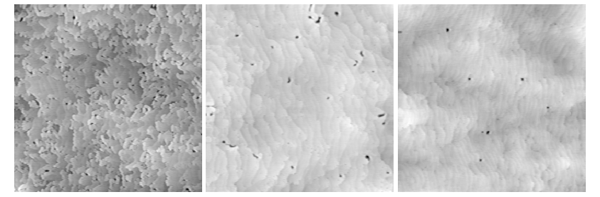
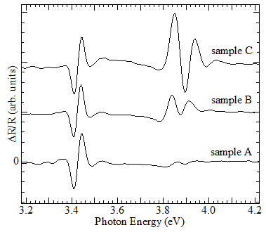
*: The details, see Takeuchi et. al The European Physical Journal -Applied Physics vol. 37, pp. 119-122 (2007).
2 : List of outcomes
_Publications
1 "Analysis of a phase factor of Franz-Keldysh oscillations in GaAs/AlGaAs heterostructures".
H. Takeuchi, Y. Yamamoto, R. Hattori, T. Ishikawa, and M. Nakayama.
IEICE Transactions on Electronics vol. E86-C, pp.2015-2021 (2003).
-photoreflectanceoceedings of the 5th Topical Workshop of Heterostructure Microelectronics, Nago, Okinawa, Japan, (2003).
# Link to the online-journal site
2 "Interference effect on the phase of Franz-Keldysh oscillations in GaAs/AlGaAs heterostructures".
H. Takeuchi, Y. Yamamoto, R. Hattori, T. Ishikawa, and M. Nakayama.
Japanese Journal of Applied Physics vol. 42, pp.6772-6778 (2003).
# Link to the online-journal site
3 "Line-shape analysis of Franz-Keldysh oscillations from a base-emitter junction in an InGaP/GaAs hetero- junction bipolar transistor structure".
H. Takeuchi, Y. Yamamoto, R. Hattori, T. Ishikawa, and M. Nakayama.
Physica E: Low-dimensional Systems and Nanostructures vol 21, pp.693-697 (2004).
-photoreflectanceoceedings of the 11th International Conference on Modulated Semiconductor Structures, Nara, Japan, (2003).
# Link to the online-journal site
4 "Determination of subband energy levels of double quantum well AlGaAs lasers by photoreflectance and self-excited electron Raman scattering".
W. Susaki, S. Ukawa, S. Yokota, N. Ohno, H. Takeuchi, Y. Yamamoto, R. Hattori, A. Shima, and Y. Mihashi.
Physica E: Low-dimensional Systems and Nanostructures vol 21, pp.793-797 (2004).
-photoreflectanceoceedings of the 11th International Conference on Modulated Semiconductor Structures, Nara, Japan, (2003).
# Link to the online-journal site
5 "Nondestructive determination of layers photoreflectanceoducing Franz-Keldysh oscillations appearing in photoreflectance spectra of heterojunction bipolar transistor structures based on their line-shape analysis.
H. Takeuchi, Y. Yamamoto, and M. Nakayama.
Journal of Applied Physics vol.96, pp.1967-1974 (2004).
# Link to the online-journal site
6 "Photovoltaic effects on Franz-Keldysh oscillations in photoreflectance spectra: application to determination of surface Fermi level and surface recombination velocity in undoped GaAs/n-type GaAs epitaxial layer structures".
H. Takeuchi, Y. Kamo, Y. Yamamoto, T. Oku, M. Totsuka, and M. Nakayama.
Journal of Applied Physics vol.97, 063708 (2005).
# Link to the online-journal site
7 "Effects of a cap layer on built-in electric fields of AlxGa1-x N/GaN heterostructures non-destructively photoreflectanceobed by Franz-Keldysh oscillations".
H. Takeuchi,Y. Yamamoto, Y. Kamo, T. Oku, and M. Nakayama.
The European Physical Journal B, vol. 52, pp.311-314 (2006).
# Link to the online-journal site
8 "High sensitivity of Franz-Keldysh oscillations in photoreflectance spectra for photoreflectanceobing morphology in AlxGa1-x N/GaN heterostructures".
H. Takeuchi,Y. Yamamoto, Y. Kamo, T. Kunii, T. Oku, S. Wakaiki, and M. Nakayama.
The European Physical Journal -Applied Physics vol. 37, pp. 119-122 (2007).
# Link to the online-journal site
3 : Posters and viewgraphs
1 "Analysis of a phase factor of Franz-Keldysh oscillations in GaAs/AlGaAs heterostructures".
H. Takeuchi, Y. Yamamoto, R. Hattori, T. Ishikawa, and M. Nakayama.
The 5th Topical Workshop of Heterostructure Microelectronics (TWHM 2003), January 21-24, 2003, Nago, Okinawa, Japan.
The abstract is here.
2 "Line-shape analysis of Franz-Keldysh oscillations from a base-emitter junction in an InGaP/GaAs hetero- junction bipolar transistor structure".
H. Takeuchi, Y. Yamamoto, R. Hattori, T. Ishikawa, and M. Nakayama.
The 11th International Conference on Modulated Semiconductor Structures (MSS11), July 14 - 18, 2003, Nara New Public Hall, Nara, Japan.
*** Poster photoreflectanceesentation: PA56 (Monday) ***
The abstract is here.